") 深度解析Xilinx FPGA的GTx的參考時鐘
深度解析Xilinx FPGA的GTx的參考時鐘
本文主要介紹Xilinx FPGA的GTx的參考時鐘。下面就從參考時鐘的模式、參考時鐘的選擇等方面進(jìn)行介紹。
參考時鐘的模式
參考時鐘可以配置為輸入模式也可以是輸出模式,但是在運(yùn)行期間不能切換。作為輸入時,用于驅(qū)動Quad 或者channel PLLs,作為輸出時,可以來自于同一個Quad中的任意一個channel。7系列的GTx只能作為輸入,而Ultra和Ultra+系列的還可以作為輸出。
作為輸入模式時,7系列和Ultra是通過50Ω連接到4/5MGTAVCC上,Ultra+是通過50Ω連接到MGTAVCC上。后端根據(jù)不同系列器件給到不同IBUFDS_GTE。
作為輸出模式時,可以配置為從OBUFDS_GTE3/4或者OBUFDS_GTE3/4_ADV輸出,UseOBUFDS_GTE3/4 when the RXRECCLKOUT is always derived from the same channel. UseOBUFDS_GTE3/4_ADV if the channel providing RXRECCLKOUT can change duringruntime.
參考時鐘的選擇
The GTP transceivers in 7 series FPGAs providedifferent reference clock input options. Clock selection and availabilitydiffers slightly from 7 series GTX/GTH transceivers in that reference clockrouting is east and west bound rather than north and south bound. 只能復(fù)用鄰近的Quad的相同半部分(一個Quad分為兩半部分)(the reference clock supplied to the PLLs in a given Quad can also besourced from the adjacent Quad in the same half of the device. A Quad locatedin the top half of the device can share its two local reference clocks with theother Quad located in the top half. Similarly, a Quad located in the bottomhalf of the device can share its two reference clocks with the other Quadlocated in the bottom half.)
The GTX/GTH transceivers in 7 series FPGAs providedifferent reference clock input options. Clock selection and availability issimilar to the Virtex-6 FPGA GTX/GTH transceivers, but the reference clockselection architecture supports both the LC tank (or QPLL) and ring oscillator(or CPLL) based PLLs. 可以復(fù)用鄰近上下兩個Quad(the reference clock for a Quad (Q(n)) can also be sourced from theQuad below (Q(n–1)) via GTNORTHREFCLK or from the Quad above (Q(n+1)) viaGTSOUTHREFCLK. For devices that support stacked silicon interconnect (SSI)technology, the reference clock sharing via GTNORTHREFCLK and GTSOUTREFCLKports is limited within its own super logic region (SLR).)
The GTH transceivers in UltraScale devices providedifferent reference clock input options. Clock selection and availability issimilar to the 7 series FPGAs GTX/GTH transceivers, but the reference clockselection architecture supports two LC tanks (or QPLL) and one ring oscillator(or CPLL) based PLLs. 可以復(fù)用鄰近的上下各兩個Quad(the reference clock for a Quad (Q(n)) can also be sourced from up totwo Quads below (Q(n–1) or Q(n-2)) via GTNORTHREFCLK or from up to two Quadsabove (Q(n+1) or Q(n+2)) via GTSOUTHREFCLK.
For devices that support stacked siliconinterconnect (SSI) technology, the reference clock sharing via GTNORTHREFCLKand GTSOUTREFCLK ports is limited within its own super logic region (SLR).)
he GTY transceivers in UltraScale devices providedifferent reference clock input options. Clock selection and availability issimilar to the 7 series FPGAs GTX/GTH transceivers, but the reference clockselection architecture supports two LC tanks (or QPLL) and one ring oscillator(or CPLL) based PLLs. 可以復(fù)用鄰近的上下各兩個Quad.
對應(yīng)的時鐘源有如下區(qū)分:
① GTP對應(yīng)的Each GTPE2_COMMON in a Quad hasfour clock inputs available:
- Two local referenceclock pin pairs, GTREFCLK0 or GTREFCLK1
- Two reference clock pinpairs from the other Quad situated in the same half of the device
② 7系列的GTX/GTH對應(yīng)的Each GTX/GTH transceiver channel ina Quad has six clock inputs available:
- Two local referenceclock pin pairs, GTREFCLK0 or GTREFCLK1
- Two reference clock pinpairs from the Quads above, GTSOUTHREFCLK0 or GTSOUTHREFCLK1
- Two reference clocks pinpairs from the Quads below, GTNORTHREFCLK0 or GTNORTHREFCLK1
③ Ultra和Ultra+系列的GTx對應(yīng)的transceiver channel in a Quad hassix clock inputs available:
- Two local referenceclock pin pairs, GTREFCLK0 or GTREFCLK1
- Two reference clock pinpairs from the Quads above, GTSOUTHREFCLK0 or GTSOUTHREFCLK1
- Two reference clocks pinpairs from the Quads below, GTNORTHREFCLK0 or GTNORTHREFCLK1
④ 針對Ultra和Ultra+系列的參考時鐘源不是10個的原因詳見UG576和UG578。
QPLL/CPLL
QPLL的質(zhì)量比CPLL好,最好使用QPLL。
REFCLK
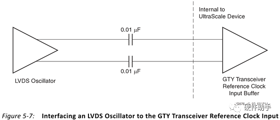
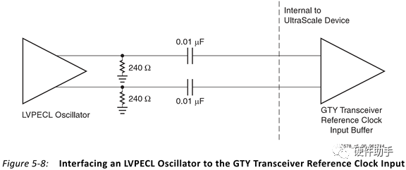
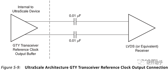
REFCLK的電平標(biāo)準(zhǔn)為LVDS或者LVPECL,都必須有AC耦合電容,電容的作用如下:
① Blocking a DC current betweenthe oscillator and the GTY transceiver Quad dedicated clock input pins (which reduces the power consumptionof both parts as well).
② Common mode voltage independence.
③ The AC coupling capacitor formsa high-pass filterwith the on-chip termination that attenuates a wander of the reference clock.
當(dāng)輸入電平為LVPECL時,需進(jìn)行直流偏置,偏置電阻的值優(yōu)先滿足晶振的要求。
當(dāng)輸入電平為LVDS時,The nominal range is 250 mV–2000 mV and the nominal value is 1200mV.
When multiple clock pins are used, an external buffer can be used to drive them from the same oscillator. 當(dāng)同一個quad使用了不用的時鐘輸入引腳時,可以使用外部時鐘buffer提供外同步時鐘!!!
編輯:hfy
-
FPGA
+關(guān)注
關(guān)注
1643文章
21960瀏覽量
614059 -
Xilinx
+關(guān)注
關(guān)注
73文章
2182瀏覽量
124342 -
GTX
+關(guān)注
關(guān)注
0文章
36瀏覽量
11051 -
參考時鐘
+關(guān)注
關(guān)注
0文章
6瀏覽量
3043
發(fā)布評論請先 登錄
XILINX XCZU67DR FPGA完整原理圖
gtx是光纖嗎
Xilinx Ultrascale系列FPGA的時鐘資源與架構(gòu)解析
詳解Xilinx的10G PCS PMA IP

xilinx FPGA IOB約束使用以及注意事項(xiàng)
將ADC32RF42 EVM與xilinx ZC706開發(fā)板直接相連,JESD204B時鐘無法建鏈成功,為什么?
采用Xilinx FPGA的AFE79xx SPI啟動指南

【米爾-Xilinx XC7A100T FPGA開發(fā)板試用】+04.SFP之Aurora測試(zmj)
Xilinx 7系列FPGA PCIe Gen3的應(yīng)用接口及特性
FPGA加速深度學(xué)習(xí)模型的案例
深度解析linux時鐘子系統(tǒng)


 工商網(wǎng)監(jiān)
評論