") 信號尋跡器/信號發(fā)生器(英文),Pulse-Generator & Signal-Tracer
信號尋跡器/信號發(fā)生器(英文),Pulse-Generator & Signal-Tracer
信號尋跡器/信號發(fā)生器(英文),Pulse-Generator & Signal-Tracer
關(guān)鍵字:信號尋跡器/信號發(fā)生器
Circuit diagram
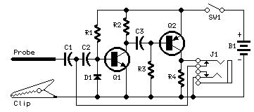
Parts:
R1 1M 1/4W Resistor
R2,R4 2K7 1/4W Resistors
R3 150K 1/4W Resistor
C1 2n2 630V Ceramic or Polyester Capacitor (See Notes)
C2,C3 4n7 63V Ceramic or Polyester Capacitors
D1 1N4148 75V 150mA Diode
Q1 BC547 45V 100mA NPN Transistor
Q2 BC557 45V 100mA PNP Transistor
SW1 SPST miniature Slider Switch (See Notes)
J1 Stereo switched 3mm. Jack socket (See Notes)
Probe Metal Probe 3 to 5 cm. long
Clip Miniature Crocodile Clip
B1 1.5V Battery (AA or AAA cell etc.)
Device purpose:
This simple circuit generates narrow pulses at about 700-800Hz frequency. The pulses, containing harmonics up to the MHz region, can be injected into audio or radio-frequency stages of amplifiers, receivers and the like for testing purposes. A high-pitched tone can be heard from the speaker of the device under test when all is working properly. The clip must be connected to the ground of the device under test, touching with the probe the different stages of the circuit, starting from the last stage and going up towards the first. When the tone is no longer heard, the defective stage has been found.
Connecting an earclip or headphone to J1, the circuit will automatically change into a two-stage amplifier and any audio signal coming from the device under test and picked-up by the probe will be heard through the headphones. The testing of a circuit should be made in the reverse manner, i.e. starting from the first stage and going down until the last stage. When nothing is heard, the defective stage has been found.
Circuit operation:
Q1 & Q2 form a complementary astable multivibrator, whose operating frequency is set mainly by R3, C2 & C3 values. Output pulses are taken at Q2 Collector and applied to the probe by means of decoupling capacitor C1. D1 provides a symmetrical shape for the output waveform.
If an earclip or headphone jack is plugged into J1, the connection from Q2 Collector and C1-C2 is broken by the switch incorporated into J1: in this case the circuit becomes a two-stage amplifier.
Notes:
If you intend to use the circuit to test valve operated devices C1 must be a 630V type. Working with low voltage supply transistor devices the voltage of C1 can be lowered to 63 or 100V.
If instead of a short probe, you intend to connect the circuit to the device under test by means of a piece of wire longer than a few centimeters, a small ceramic capacitor (470 to 1000pF) should be added in parallel to D1 to prevent unwanted RF oscillation.
Current drawing when in Pulse-Generator mode is about 60?μA & 1.2mA when in Signal-Tracer mode operation. Therefore SW1 can be omitted, provided that the earclip or headphones are unplugged when the circuit is unused.
J1 is a stereo switched jack socket wired to obtain a series connection of the two earpieces forming a stereo headphone. In this manner the circuit is loaded with a higher impedance and sensitivity will be improved.
Therefore, the higher the load impedance the more sensitive the Signal-Tracer. In any case, common 32 Ohm impedance mini-headphones suitable for walkman sets will work fine.
A crystal (high impedance) earpiece is a good solution, provided you substitute J1 with a mono switched jack socket.
The entire circuit can be easily fitted into a pen-like enclosure, with the probe protruding like a nib.
Author: RED Free Circuit Designs
聲明:本文內(nèi)容及配圖由入駐作者撰寫或者入駐合作網(wǎng)站授權(quán)轉(zhuǎn)載。文章觀點僅代表作者本人,不代表電子發(fā)燒友網(wǎng)立場。文章及其配圖僅供工程師學(xué)習(xí)之用,如有內(nèi)容侵權(quán)或者其他違規(guī)問題,請聯(lián)系本站處理。
舉報投訴
發(fā)布評論請先 登錄
相關(guān)推薦
熱點推薦
開機(jī)報錯失鎖?怎么回事?今天就帶大家沉浸式體驗N5171B信號發(fā)生器維修過程 #信號發(fā)生器維修 #電工維修
信號發(fā)生器
安泰儀器維修
發(fā)布于 :2025年05月23日 19:00:29
DG535脈沖信號發(fā)生器出現(xiàn)偏置故障,福爾摩斯&外科醫(yī)生工程師就要上場了!#維修 #信號發(fā)生器
信號發(fā)生器
安泰儀器維修
發(fā)布于 :2025年04月21日 18:29:27
信號發(fā)生器PM調(diào)制信號設(shè)置
信號發(fā)生器與PM調(diào)制的重要性 在現(xiàn)代通信技術(shù)和電子實驗中,信號發(fā)生器已成為測試和驗證設(shè)備中必不可少的工具。無論是在科研實驗、產(chǎn)品開發(fā),還是設(shè)備調(diào)試過程中,
信號發(fā)生器的組成元件
信號發(fā)生器是電子測試和實驗過程中常用的電子儀器,能夠輸出各種高品質(zhì)、高性能的波形。它主要由多個關(guān)鍵元件和組件構(gòu)成,這些元件共同協(xié)作,實現(xiàn)信號的生成、調(diào)節(jié)和輸出。本文將詳細(xì)探討信號

DDS信號發(fā)生器支持單通道50個正弦載波!#信號發(fā)生器 #AWG #DDS
信號發(fā)生器
虹科衛(wèi)星與無線電通信
發(fā)布于 :2024年12月23日 18:03:30

DDS信號發(fā)生器在量子研究中的應(yīng)用——控制聲光偏轉(zhuǎn)器/調(diào)制器 #DDS #信號發(fā)生器 #量子 #聲光偏轉(zhuǎn)器
信號發(fā)生器
虹科衛(wèi)星與無線電通信
發(fā)布于 :2024年11月29日 15:47:20
泰克信號發(fā)生器的半導(dǎo)體測試應(yīng)用
隨著半導(dǎo)體技術(shù)的飛速發(fā)展,半導(dǎo)體測試變得越來越復(fù)雜和具有挑戰(zhàn)性。在這種情況下,信號發(fā)生器作為測試設(shè)備的一個組成部分,扮演了越來越重要的角色。泰克信號發(fā)生器是一種高性能的

任意波形發(fā)生器的基本架構(gòu)
任意波形發(fā)生器(Arbitrary Waveform Generator,AWG)是從信號發(fā)生器演進(jìn)過來的一款信號源,其架構(gòu)的設(shè)計旨在提供高
文氏橋信號發(fā)生器的工作原理和結(jié)構(gòu)
文氏橋信號發(fā)生器是一種基于文氏橋電路的信號發(fā)生器,它能夠產(chǎn)生穩(wěn)定且頻率可調(diào)的正弦波信號。以下是對文氏橋信


新手入門教程|信號發(fā)生器也能輸出高壓大電流信號!#信號發(fā)生器 #信號源 #高壓信號 #電子工程師 #電子基礎(chǔ)
電流信號發(fā)生器
安泰小課堂
發(fā)布于 :2024年09月24日 18:20:28
泰克信號發(fā)生器測量信號幅度
在電子工程領(lǐng)域,準(zhǔn)確測量信號幅度是至關(guān)重要的環(huán)節(jié)。泰克信號發(fā)生器以其卓越的性能和精準(zhǔn)的輸出,成為眾多工程師信賴的工具。今天,我們就來探討一下如何使用泰克信號
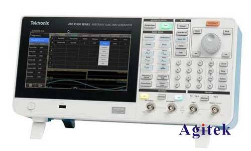
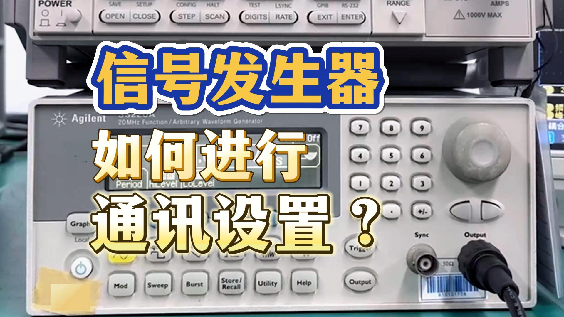
信號發(fā)生器如何進(jìn)行通訊設(shè)置#信號發(fā)生器#通訊設(shè)置#示波器#網(wǎng)絡(luò)分析儀#示波器維修
信號發(fā)生器
安泰儀器維修
發(fā)布于 :2024年09月11日 17:44:09
信號發(fā)生器的運用介紹
信號發(fā)生器是一種能供應(yīng)各種頻率、波形和輸出電平電信號的設(shè)備。在測量各種電信系統(tǒng)或電信設(shè)備的振幅特性、頻率特性、傳輸特性及其它電參數(shù)時,以及測量元器件的特性與參數(shù)時,用作測試的信號源或激
PWM信號發(fā)生器的作用有哪些
PWM(Pulse Width Modulation),即脈沖寬度調(diào)制,是一種利用微處理器的數(shù)字輸出來對模擬電路進(jìn)行控制的非常有效的技術(shù)。PWM信號發(fā)生器作為這一技術(shù)的核心設(shè)備,其作用
什么是AWG?AWG和其他信號發(fā)生器的差別
任意波形發(fā)生器(Arbitrary Waveform Generator, 以下簡稱“AWG”)是從信號發(fā)生器演進(jìn)過來的一款信號源。1988


 工商網(wǎng)監(jiān)
評論