") 英特爾技術(shù)與制造前沿研究項(xiàng)目
英特爾技術(shù)與制造前沿研究項(xiàng)目

還有哪些制勝未來(lái)的殺手锏?
獨(dú)家揭秘,就在知IN
英特爾技術(shù)與制造前沿研究項(xiàng)目
Intel’s Components Research teamfund sand works with universities and academic research consortia on forward-looking research topics such as Spintronics, and also on the understanding of fundamental science which is the basis of these forward-looking research.
英特爾前沿研究部門(mén)資助多家大學(xué)院校和學(xué)術(shù)機(jī)構(gòu),共同開(kāi)展多種前沿研究課題,比如自旋電子以及這些前沿研究的基礎(chǔ)科學(xué)。
英特爾高級(jí)院士、技術(shù)與制造事業(yè)部制程架構(gòu)與集成總監(jiān)Mark T. Bohr
解讀英特爾前沿研究項(xiàng)目
1Nanowire transistorsare being explored as a future option because the nanowire structure provides improves channel electrostatics that can enable further transistor gate length scaling.
納米線晶體管被認(rèn)為是未來(lái)技術(shù)的一種選擇,因?yàn)榧{米線的結(jié)構(gòu)可提供改進(jìn)通道靜電,從而進(jìn)一步實(shí)現(xiàn)晶體管柵極長(zhǎng)度的微縮。
2Silicon has always been the material used in MOSFET channels, butIII-V materialssuch as GaAs and InP have improved carrier mobility that can provide higher performance or the ability to operate transistors at lower voltage for lower active power.
硅是MOSFET通道中經(jīng)常使用的材料,但是III-V 材料(如砷化鎵和磷化銦)改進(jìn)了載流子遷移率,從而提供更高的性能或者能夠在更低的電壓和更低的有功功耗下運(yùn)行晶體管。
33D stackingof silicon die can provide system integration opportunities to mix different technologies into a small form factor.
硅晶片的3D堆疊有機(jī)會(huì)實(shí)現(xiàn)系統(tǒng)集成,以便把不同的技術(shù)混裝到一個(gè)很小的地方。
4A variety ofdense memoryoptions, including volatile and non-volatile memory, are being explored and developed.
多種不同的高密度內(nèi)存選擇,其中包括易失性和非易失性存儲(chǔ)技術(shù),正在探索和開(kāi)發(fā)中。
5Scaling interconnectsis just as important as scaling transistors on advanced process technologies. Novel materials and patterning techniques are being explored to enable dense interconnects.
對(duì)于精尖制程工藝來(lái)說(shuō),微縮互聯(lián)和微縮晶體管一樣重要。新的材料和圖案成形技術(shù)正在探索中,以支持高密度互聯(lián)。
6Extreme Ultraviolet(EUV) lithography using a 13.5 nm wavelength is being developed to enable better scaling as today’s 193nm wavelength tools reach their scaling limit.
極紫外(EUV)光刻技術(shù):采用13.5納米波長(zhǎng)。由于當(dāng)今的193納米波長(zhǎng)工具已達(dá)到其微縮極限,該技術(shù)正在研發(fā)中以實(shí)現(xiàn)進(jìn)一步的微縮。
7
Spintronicsis a beyond-CMOS technology that promises very dense and low power circuits that are an option when CMOS can no longer be scaled.
自旋電子是一種超越CMOS的技術(shù),當(dāng)CMOS無(wú)法再進(jìn)行微縮的時(shí)候,這是一種選擇,可提供非常密集和低功耗的電路。
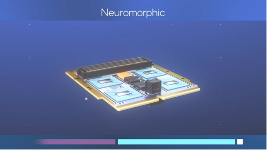
8Neuromorphic computingis a different processor design and architecture approach for performing some computing functions with much better power efficiency than today’s computers.
神經(jīng)元計(jì)算是一種不同的處理器設(shè)計(jì)和架構(gòu),能夠以比當(dāng)前計(jì)算機(jī)高得多的能效執(zhí)行某些計(jì)算功能。
-
英特爾
+關(guān)注
關(guān)注
61文章
10196瀏覽量
174680 -
納米線晶體管
+關(guān)注
關(guān)注
0文章
1瀏覽量
1316
原文標(biāo)題:首次揭秘:英特爾制勝未來(lái)的半導(dǎo)體前沿技術(shù)儲(chǔ)備
文章出處:【微信號(hào):Intelzhiin,微信公眾號(hào):知IN】歡迎添加關(guān)注!文章轉(zhuǎn)載請(qǐng)注明出處。
發(fā)布評(píng)論請(qǐng)先 登錄
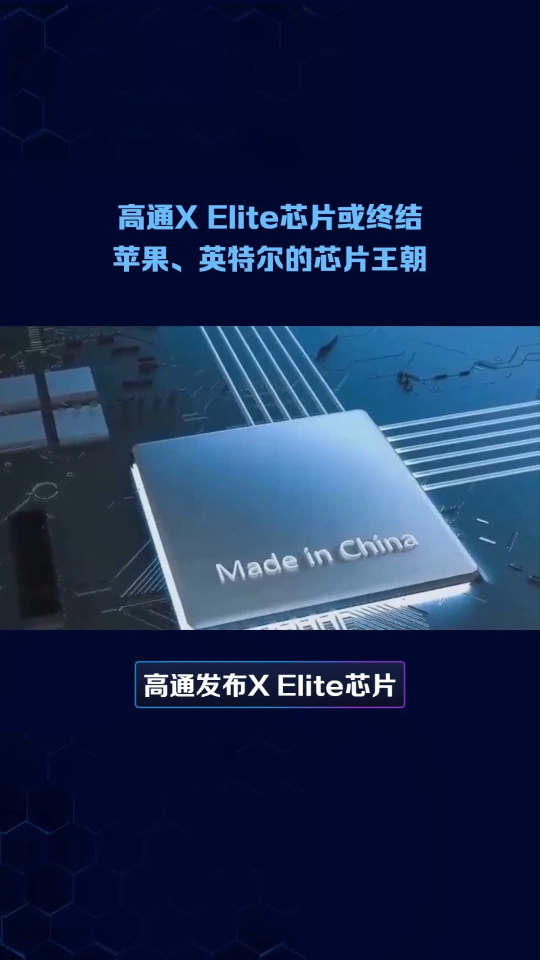
#高通 #英特爾 #Elite 高通X Elite芯片或終結(jié)蘋(píng)果、英特爾的芯片王朝
英特爾將在2014年推出14納米處理器芯片
英特爾轉(zhuǎn)型移動(dòng)領(lǐng)域難言樂(lè)觀
【AD新聞】英特爾解讀全球晶體管密度最高的制程工藝
為什么選擇加入英特爾?
英特爾重新思考解決芯片短缺的常用基板
英特爾在前沿研究領(lǐng)域的諸多洞察與成果
英特爾技術(shù)制造集團(tuán)將拆分 英特爾放棄智能眼鏡Vaunt
2022英特爾中國(guó)研究院探索創(chuàng)新日,探索科技創(chuàng)新無(wú)窮奧秘
「前沿技術(shù)」英特爾以硅基技術(shù)成功制造量子芯片
「前沿技術(shù)」英特爾以硅基技術(shù)成功制造量子芯片
一起云逛展,帶你感受英特爾開(kāi)源前沿技術(shù)的魅力!
2023英特爾on技術(shù)創(chuàng)新大會(huì):英特爾研究院展示多項(xiàng)技術(shù)“魔法”


 工商網(wǎng)監(jiān)
評(píng)論