 電子發燒友App


1 概述
本設計已實用于國家863計劃“可擴展到T比特的高性能IPv4/v6路由器基礎平臺及實驗系統”項目中。其主要功能是對主控部分的FPGA讀取Flash進行控制。
在本項目中,主控部分的FPGA在重啟時需要從Flash中下載初始化程序。當下載完成后,FPGA仍會根據需要從Flash相應地址讀取數據。這就要求在FPGA和Flash之間有一塊控制邏輯來控制對Flash的讀取。本設計就是完成的對這塊控制邏輯的具體實現。
本文用VHDL語言在CPLD內部編程將其實現。本文第2節給出用VHDL語言在CPLD內部編程實現Flash讀取的過程,第3節對全文進行概括總結。
2 實現
2.1 器件的選擇
我們選用Xilinx公司XC9500XL 3.3V ISP 系列XC95288XL-7TQ144I芯片。XC95288xl是一個3.3V的低電壓、高效的CPLD,在通信和計算機系統中的有廣泛的應用。它包含16個54V18個功能塊,提供了6400個可用的門電路,這些門電路的傳播延時為6ns.
對于Flash,項目中選擇了Intel公司的Intel StrataFlash系列的256-Mbit J3型Flash.其數據寬度可分別支持8位或者16位。
2.2 實現中的問題及解決方法
項目中選用的Flash的輸出為16位,而向FPGA輸出的數據為32位,因此產了數據寬度不匹配的問題,解決的方法有兩種:
第一 使用兩塊相同的Flash,分別將其輸出的數據送入FPGA接口的高16位和低16位;其缺點是需要增加一塊Flash,從而成本增加。
第二 采用降低讀取速度的方法,把從一塊Flash中連續兩次讀取的16位數據拼接起來,組成一組32位的數據后送入FPGA接口。
出于對成本和復雜度的考慮,在此設計中我們采取了第二種方法加以實現。
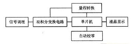
2.3 基本設計模塊圖

2.4 用VHDL進行實現(注:實體部分定義可分別參見模塊圖中的劃分)
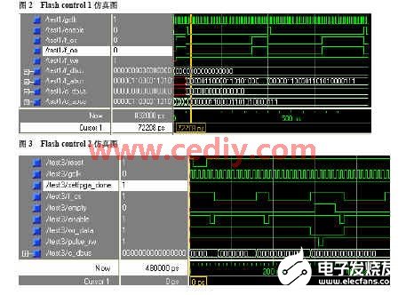
Flash control 1
process(reset,gclk)
begin
if reset =‘0’ then
count_reset 《=‘0’;
elsif gclk‘event and gclk =’1‘ then
count_reset 《= not(count(4) and count(3) and count(2));
end if;
end process;
process(count_reset,gclk)
begin
if count_reset =’0‘ then
count 《=(others =》’0‘);
elsif gclk’event and gclk =‘1’ then
count 《=count +1;
end if;
end process;
process(count_reset,reset,enable)
begin
if reset =‘0’ then
F_CS 《=‘1’;
F_OE 《=‘1’;
F_WE 《=‘1’;
elsif count_reset =‘0’ then
F_CS 《= ‘1’;
F_OE 《= ‘1’;
F_WE 《= ‘1’;
elsif enable‘event and enable =’1‘ then
F_Abus 《= C_Abus;
F_CS 《= ’0‘;
F_OE 《= ’0‘;
F_WE 《= ’1‘;
C_Dbus 《= F_Dbus;
end if;
end process;
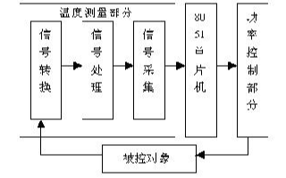
Flash control 2
d_count_rst 《= not(d_count(1) and (not d_count(0)) and empty);
sig_WD 《= not(d_count(1) and (not d_count(0)));
WR_DATA 《= sig_WD;
process(gclk,d_count)
begin
if reset =’0‘ then
d_count 《= ’1‘;
elsif F_CS = ’1‘ then
d_count1 《= not d_count1 ;
if gclk’event and gclk =‘1’ then
d_count2 《= d_count1;
d_count 《= d_count2;
end if;
end if;
end process;
process(reset,d_count,C_Dbus)
begin
if reset = ‘0’ then
data_adder 《= (others =》‘0’);
elsif d_count‘event and d_count = ’0‘ then
data_adder(31 downto 16) 《= C_Dbus;
elsif d_count’event and d_count = ‘1’ then
data_adder(15 downto 0) 《= C_Dbus;
end if;
end process;
enable 《= enable1 and enable2;
process(reset,d_count,F_CS)
begin
if reset = ‘0’ or F_CS = ‘0’ then
enable1 《= ‘1’;
enable2 《= ‘1’;
elsif d_count‘event then
if gclk’event and gclk =‘1’ then
enable1 《= ‘0’;
enable2 《= not enable1;
end if;
end if;
end process;
process(reset,F_CS)
begin
if reset = ‘0’ then
address《= X“400000”;
elsif F_CS = ‘1’ then
C_Abus 《= address;
address 《= adderss +1;
end if;
end process;
process(reset,F_CS)
begin
if reset = ‘0’ then
address《= X“400000”;
data_adder 《=(others =》‘0’);
elsif F_CS = ‘1’;
address 《= adderss +1;
end if;
end process;
process(d_count2,F_CS)
begin
if F_CS = ‘0’ then
enable1 《= ‘1’;
enable 《= ‘1’;
elsif d_count2 = “00” or d_count2 = “01” then
enable 《= ‘0’;
end if;
end process;
process(gclk,sig_WD)
begin
if sig_WD = ‘1’ then
Pulse_RW 《=‘1’;
elsif gclk‘event and gclk =’1‘ then
W_D1 《= sig_WD;
W_D2 《= W_D1;
if empty =’0‘ then
data_adder1 《= data_adder;
Pulse_RW 《= (W_D1 or (not W_D2));
end if;
end if;
end process;
(注:此程序在Xilinx公司的ISE6.2i環境下用VHDL編程實現,其仿真波形見下圖)
3 結束語
在實際應用中,以此CPLD對Flash的讀取進行控制。仿真結果及最后的實際調試都表明該設計符合項目的要求。在程序中通過對讀取的記數控制,本設計可以在不增加Flash片數的情況下支持16/32/64位的數據輸出寬度。可以節約一定的成本,具有相當的靈活性和實用性。
責任編輯:gt


 工商網監
工商網監
評論