

| Regulated outputs (#) | 6 |
| Vin (Min) (V) | 1.5 |
| Vin (Max) (V) | 6.5 |
| Iout (Max) (A) | 0.6 |
| Rating | Catalog |
| LDO | 4 |
| Iq (Typ) (mA) | 1.25 |
| Features | I2C Control |
| Shutdown current (ISD) (Typ) (uA) | 18 |
| Switching frequency (Typ) (kHz) | 2250 |
| Configurability | Hardware configurable |
- Up to 95% Efficiency
- Output Current for DCDC Converters 2 × 0.6 A
- Two Selectable Fixed Output Voltages 1 V and
1.2 V for DCDC2 - VIN Range for DCDC Converters From 2.5 V to 6 V
- 2.25-MHz Fixed-Frequency Operation
- Power Save Mode at Light Load Current
- 180° Out-of-Phase Operation
- Output Voltage Accuracy in PWM Mode ±1%
- Low Ripple PFM Mode
- Total Typical 32-μA Quiescent Current for Both
DC-DC Converters - 100% Duty Cycle for Lowest Dropout
- 2 General-Purpose 400 mA High PSRR LDOs
- 2 General-Purpose 200 mA High PSRR LDOs
- VIN Range for LDOs From 1.5 V to 6.5 V
- Digital Voltage Selection for the LDOs
- I2C Compatible Interface
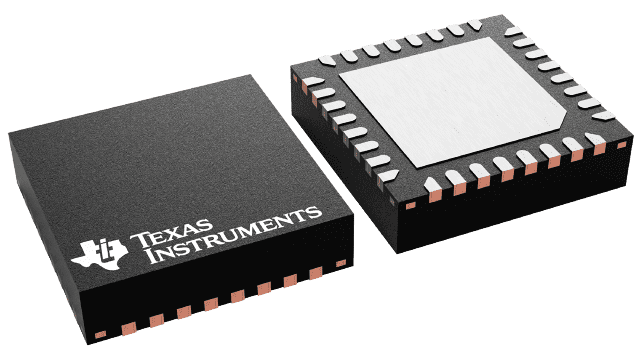
- Available in a 4 mm × 4 mm 32-Pin QFN Package
The TPS65055 device is an integrated Power Management IC for applications powered by one Li-Ion or Li-Polymer cell, which require multiple power rails.
The TPS65055 provides two highly efficient, 2.25 MHz step-down converters targeted at providing the core voltage and I/O voltage in a processor-based system. Both step-down converters enter a low power mode at light load for maximum efficiency across the widest possible range of load currents.
For low noise applications the device can be forced into fixed frequency PWM mode using the I2C compatible interface. In shutdown mode, current consumption is reduced to less than 1 μA.
The device allows the use of small inductors and capacitors to achieve a small solution size.
The TPS65055 provides an output current of up to 0.6 A on each DC-DC converter.
The TPS65055 also integrates two 400-mA LDO and two 200-mA LDO voltage regulators, which can be turned on/off using separate enable pins on each LDO. Each LDO operates with an input voltage range from 1.5 V to 6.5 V allowing them to be supplied from one of the step-down converters or directly from the main battery. Two digital input pins are used to set the output voltage of the LDOs from a set of 9 different combinations for LDO1 to LDO4. Additionally, the converters can be controlled by an I2C compatible interface.
The TPS65055 is available in a small 32-pin leadless package (4 mm × 4 mm QFN) with a 0.4-mm pitch.


