--- 產(chǎn)品詳情 ---
Number of channels (#) | 2 |
Power switch | MOSFET, IGBT |
Peak output current (A) | 4 |
Input VCC (Min) (V) | 4 |
Input VCC (Max) (V) | 15 |
Features | Enable Pin |
Operating temperature range (C) | -40 to 125 |
Rise time (ns) | 20 |
Fall time (ns) | 15 |
Prop delay (ns) | 25 |
Input threshold | CMOS, TTL |
Channel input logic | Inverting |
Input negative voltage (V) | 0 |
Rating | Automotive |
Driver configuration | Dual inputs |
- Qualified for Automotive Applications
- AEC-Q100 Qualified With the Following Results:
- Device Temperature Grade 1: –40°C to +125°C Ambient Operating Temperature Range
- Device HBM ESD Classification Level 2
- Device CDM ESD Classification Level C6
- Industry-Standard Pinout
- Enable Functions for Each Driver
- High-Current Drive Capability of ±4 A
- Unique Bipolar and CMOS True Drive Output Stage Provides High Current at MOSFET Miller Thresholds
- Inputs Independent of Supply Voltage Compatible With TTL and CMOS
- 20-ns Typical Rise and 15-ns Typical Fall Times With 1.8-nF Load
- Typical Propagation Delay Times of 25ns With Input Falling and 35ns With Input Rising
- 4-V to 15-V Supply Voltage
- Dual Outputs Can Be Paralleled for Higher Drive Current
- Available in Thermally Enhanced MSOP PowerPAD Package
- Rated From –40°C to +125°C
All trademarks are the property of their respective owners.
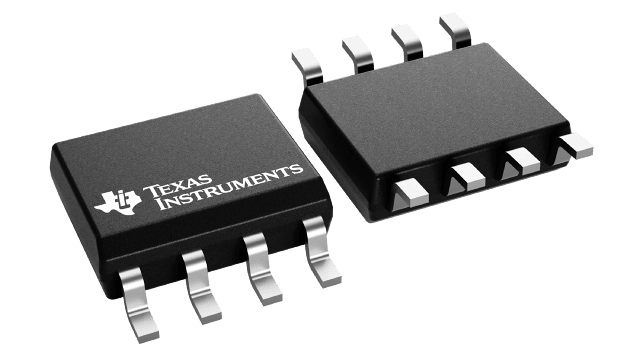
The UCC2742x-Q1 family of devices are high-speed dual MOSFET drivers capable of delivering large peak currents into capacitive loads. Two standard logic options are offered: dual inverting and dual noninverting drivers. They are offered in the standard 8-pin SOIC (D) package. The thermally enhanced 8-pin PowerPAD Package MSOP package (DGN) drastically lowers the thermal resistance to improve long-term reliability.
Using a design that inherently minimizes shoot-through current, these drivers deliver 4-A current where it is needed most, at the Miller plateau region, during the MOSFET switching transition. A unique bipolar and MOSFET hybrid output stage in parallel also allows efficient current sourcing and sinking at low supply voltages.
The UCC2742x-Q1 provide enable (ENBL) functions to have better control of the operation of the driver applications. ENBA and ENBB are implemented on pins 1 and 8, which were previously left unused in the industry standard pinout. They are internally pulled up to VDD for active-high logic and can be left open for standard operation.
For all available packages, see the orderable addendum at the end of the data sheet.為你推薦
-
TI數(shù)字多路復(fù)用器和編碼器SN54HC1512022-12-23 15:12
-
TI數(shù)字多路復(fù)用器和編碼器SN54LS1532022-12-23 15:12
-
TI數(shù)字多路復(fù)用器和編碼器CD54HC1472022-12-23 15:12
-
TI數(shù)字多路復(fù)用器和編碼器CY74FCT2257T2022-12-23 15:12
-
TI數(shù)字多路復(fù)用器和編碼器SN74LVC257A2022-12-23 15:12
-
TI數(shù)字多路復(fù)用器和編碼器SN74LVC157A2022-12-23 15:12
-
TI數(shù)字多路復(fù)用器和編碼器SN74ALS258A2022-12-23 15:12
-
TI數(shù)字多路復(fù)用器和編碼器SN74ALS257A2022-12-23 15:12
-
TI數(shù)字多路復(fù)用器和編碼器SN74ALS157A2022-12-23 15:12
-
TI數(shù)字多路復(fù)用器和編碼器SN74AHCT1582022-12-23 15:12
-
如何利用運(yùn)算放大器設(shè)計(jì)振蕩電路?2023-08-09 08:08
使用運(yùn)算放大器設(shè)計(jì)振蕩電路運(yùn)算放大器的工作原理發(fā)明運(yùn)算放大器的人絕對是天才。中間兩端接上電源,當(dāng)同相輸入大于反相輸入,右側(cè)就會輸出(接近)電源電壓(Vcc),如果反過來小于同相輸入,則輸出0V(負(fù)電源)電壓。在輸出端接上燈泡,假設(shè)我想控制燈泡循環(huán)亮滅,那就需要一會輸出高電平點(diǎn)亮,一會輸出低電平熄滅。也就是我需要讓左邊能自動變化大小,就能實(shí)現(xiàn)控制燈泡。如何讓電2017瀏覽量 -
【PCB設(shè)計(jì)必備】31條布線技巧2023-08-03 08:09
相信大家在做PCB設(shè)計(jì)時(shí),都會發(fā)現(xiàn)布線這個(gè)環(huán)節(jié)必不可少,而且布線的合理性,也決定了PCB的美觀度和其生產(chǎn)成本的高低,同時(shí)還能體現(xiàn)出電路性能和散熱性能的好壞,以及是否可以讓器件的性能達(dá)到最優(yōu)等。在上篇內(nèi)容中,小編主要分享了PCB線寬線距的一些設(shè)計(jì)規(guī)則,那么本篇內(nèi)容,將針對PCB的布線方式,做個(gè)全面的總結(jié)給到大家,希望能夠?qū)︷B(yǎng)成良好的設(shè)計(jì)習(xí)慣有所幫助。1走線長度1672瀏覽量 -
電動汽車直流快充方案設(shè)計(jì)【含參考設(shè)計(jì)】2023-08-03 08:08
大功率直流充電系統(tǒng)架構(gòu)大功率直流充電設(shè)計(jì)標(biāo)準(zhǔn)國家大功率充電標(biāo)準(zhǔn)“Chaoji”技術(shù)標(biāo)準(zhǔn)設(shè)計(jì)目標(biāo)是未來可實(shí)現(xiàn)電動汽車充電5分鐘行駛400公里。“Chaoji”技術(shù)標(biāo)準(zhǔn)主要設(shè)計(jì)參數(shù)如下:最大電壓:目前1000V(可擴(kuò)展到1500V);最大電流:帶冷卻系統(tǒng)500A(可擴(kuò)展到600A);不帶冷卻系統(tǒng)150-200A;最大功率:900KW。大功率直流充電系統(tǒng)架構(gòu)大功率 -
Buck電路的原理及器件選型指南2023-07-31 22:28
Buck電路工作原理電源閉合時(shí)電壓會快速增加,當(dāng)斷開時(shí)電壓會快速減小,如果開關(guān)速度足夠快的話,是不是就能把負(fù)載,控制在想要的電壓值以內(nèi)呢?假設(shè)12V降壓到5V,也就意味著,MOS管開關(guān)需要42%時(shí)間導(dǎo)通,58%時(shí)間斷開。當(dāng)42%時(shí)間MOS管導(dǎo)通時(shí),電感被充磁儲能,同時(shí)對電容進(jìn)行充電,給負(fù)載提供電量。當(dāng)58%時(shí)間MOS管斷開時(shí),由于電感上的電流不能突變,電路通 -
100W USB PD 3.0電源2023-07-31 22:27
-
千萬不要忽略PCB設(shè)計(jì)中線寬線距的重要性2023-07-31 22:27
想要做好PCB設(shè)計(jì),除了整體的布線布局外,線寬線距的規(guī)則也非常重要,因?yàn)榫€寬線距決定著電路板的性能和穩(wěn)定性。所以本篇以RK3588為例,詳細(xì)為大家介紹一下PCB線寬線距的通用設(shè)計(jì)規(guī)則。要注意的是,布線之前須把軟件默認(rèn)設(shè)置選項(xiàng)設(shè)置好,并打開DRC檢測開關(guān)。布線建議打開5mil格點(diǎn),等長時(shí)可根據(jù)情況設(shè)置1mil格點(diǎn)。PCB布線線寬01布線首先應(yīng)滿足工廠加工能力,1763瀏覽量 -
基于STM32的300W無刷直流電機(jī)驅(qū)動方案2023-07-06 10:02
如何驅(qū)動無刷電機(jī)?近些年,由于無刷直流電機(jī)大規(guī)模的研發(fā)和技術(shù)的逐漸成熟,已逐步成為工業(yè)用電機(jī)的發(fā)展主流。圍繞降低生產(chǎn)成本和提高運(yùn)行效率,各大廠商也提供不同型號的電機(jī)以滿足不同驅(qū)動系統(tǒng)的需求。現(xiàn)階段已經(jīng)在紡織、冶金、印刷、自動化生產(chǎn)流水線、數(shù)控機(jī)床等工業(yè)生產(chǎn)方面應(yīng)用。無刷直流電機(jī)的優(yōu)點(diǎn)與局限性優(yōu)點(diǎn):高輸出功率、小尺寸和重量、散熱性好、效率高、運(yùn)行速度范圍寬、低 -
上新啦!開發(fā)板僅需9.9元!2023-06-21 17:43
-
參考設(shè)計(jì) | 2KW AC/DC數(shù)字電源方案2023-06-21 17:43
-
千萬不能小瞧的PCB半孔板2023-06-21 17:34