| Resolution (Bits) | 12 |
| Number of input channels | 2 |
| Sample rate (Max) (kSPS) | 1000 |
| Interface type | SPI, Microwire (Serial I/O) |
| Architecture | SAR |
| Input type | Differential |
| Multi-channel configuration | Simultaneous Sampling |
| Rating | Catalog |
| Reference mode | Ext |
| Input range (Max) (V) | 5.5 |
| Input range (Min) (V) | 0 |
| Operating temperature range (C) | -40 to 105 |
| Power consumption (Typ) (mW) | 20 |
| Analog voltage AVDD (Min) (V) | 4.5 |
| SNR (dB) | 73.2 |
| Analog voltage AVDD (Max) (V) | 5.5 |
| INL (Max) (+/-LSB) | 1 |
| Digital supply (Min) (V) | 2.7 |
| Digital supply (Max) (V) | 5.25 |
- True Simultaneous Sampling Differential Inputs
- Guaranteed Performance from 500 kSPS to 1 MSPS
- External Reference
- Wide Input Common-Mode Voltage Range
- Single or Dual High-Speed Serial Data Outputs
- Operating Temperature Range of ?40°C to +105°C
- SPI?/QSPI?/MICROWIRE/DSP Compatible Serial Interface
Key Specifications
- Conversion Rate: 500 kSPS to 1 MSPS
- INL: ±1 LSB (Max)
- DNL: ±0.95 LSB (Max)
- SNR: 71 dBc (Min)
- THD: -72 dBc (Min)
- ENOB: 11.25 Bits (Min)
- Power Consumption at 1 MSPS
- Converting, VA = 5V, VD = 3V: 20 mW (Typ)
- Converting, VA = 5V, VD = 5V: 25 mW (Typ)
- Power-Down: 3 μW (Typ)
All trademarks are the property of their respective owners.
The ADC122S706 is a dual 12-bit, 500 kSPS to 1 MSPS simultaneous sampling Analog-to-Digital (A/D) converter. The analog inputs on both channels are sampled simultaneously to preserve their relative phase information to each other. The converter is based on a successive-approximation register architecture where the differential nature of the analog inputs is maintained from the internal track-and-hold circuits throughout the A/D converter to provide excellent common-mode signal rejection. The ADC122S706 features an external reference that can be varied from 1.0V to VA.
The ADC122S706 offers dual high-speed serial data outputs that are binary 2's complement and are compatible with several standards, such as SPI?, QSPI?, MICROWIRE, and many common DSP serial interfaces. Channel A's conversion result is outputted on DOUTA while Channel B's conversion result is outputted on DOUTB. This feature makes the ADC122S706 an excellent replacement for systems using two distinct ADCs in a simultaneous sampling application. The serial clock (SCLK) and chip select bar (CS) are shared by both channels. For lower power consumption, a single serial data output mode is externally selectable.
The ADC122S706 may be operated with independent analog (VA) and digital (VD) supplies. VA can range from 4.5V to 5.5V and VD can range from 2.7V to VA. With the ADC122S706 operating with a VA of 5V and a VD of 3V, the power consumption at 1 MSPS is typically 25 mW. Operating in power-down mode, the power consumption of the ADC122S706 decreases to 3 μW. The differential input, low power consumption, and small size make the ADC122S706 ideal for direct connection to sensors in motor control applications.
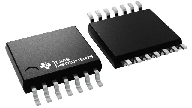
Operation is guaranteed over the industrial temperature range of ?40°C to +105°C and clock rates of 8 MHz to 16 MHz. The ADC122S706 is available in a 14-lead TSSOP package.


