| Sample rate (Max) (MSPS) | 200 |
| Resolution (Bits) | 16 |
| Number of input channels | 1 |
| Interface type | Parallel LVDS |
| Analog input BW (MHz) | 730 |
| Features | High Performance |
| Rating | Catalog |
| Input range (Vp-p) | 3 |
| Power consumption (Typ) (mW) | 2160 |
| Architecture | Pipeline |
| SNR (dB) | 75.8 |
| ENOB (Bits) | 12.1 |
| SFDR (dB) | 93 |
| Operating temperature range (C) | -40 to 85 |
| Input buffer | Yes |
- 170/200-MSPS Sample Rates
- 16-Bit Resolution, 78 dBFS Noise Floor
- SFDR = 95 dBc
- On-Chip High Impedance Analog Buffer
- Efficient DDR LVDS-Compatible Outputs
- Power-Down Mode: 70 mW
- Pin-for-Pin with ADS5483/5482/5481, 135/105/80-MSPS ADCs
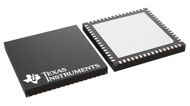
- QFN-64 PowerPAD Package (9 mm × 9 mm footprint)
- Industrial Temperature Range: –40°C to 85°C
- APPLICATIONS
- Wireless Infrastructure
- Test and Measurement Instrumentation
- Software-Defined Radio
- Data Acquisition
- Power Amplifier Linearization
- Radar
- Medical Imaging
All trademarks are the property of their respective owners
The ADS5484/ADS5485 (ADS548x) is a 16-bit family of analog-to-digital converters (ADCs) that operate from both a 5-V supply and 3.3-V supply while providing LVDS-compatible digital outputs. The ADS548x integrated analog input buffer isolates the internal switching of the onboard track and hold (T & H) from disturbing the signal source while providing a high-impedance input. An internal reference generator is provided to simplify the system design. Internal dither is available to improve SFDR. These devices are drop-in compatible to the ADS5483/5482/5481, creating a pin-compatible family from 80 – 200 MSPS. Designed for highest total ENOB, the ADS548x family has outstanding low noise performance and spurious-free dynamic range.
The ADS548x family is available in a QFN-64 PowerPAD package. The devices are built on Texas Instruments complementary bipolar process (BiCom3) and are specified over the full industrial temperature range (–40°C to 85°C).


