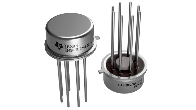
Military-grade, single, 40-V, 5-MHz, FET-input operational amplifier with QML certification
| Number of channels (#) | 1 |
| Total supply voltage (Max) (+5V=5, +/-5V=10) | 44 |
| Total supply voltage (Min) (+5V=5, +/-5V=10) | 10 |
| Rail-to-rail | No |
| GBW (Typ) (MHz) | 5 |
| Slew rate (Typ) (V/us) | 12 |
| Vos (offset voltage @ 25 C) (Max) (mV) | 5 |
| Iq per channel (Typ) (mA) | 5 |
| Vn at 1 kHz (Typ) (nV/rtHz) | 12 |
| Rating | Military |
| Operating temperature range (C) | -55 to 125 |
| Offset drift (Typ) (uV/C) | 5 |
| Input bias current (Max) (pA) | 100 |
| CMRR (Typ) (dB) | 100 |
| Output current (Typ) (mA) | 25 |
| Architecture | FET |
- Advantages
- Replace Expensive Hybrid and Module FET Op Amps
- Rugged JFETs Allow Blow-Out Free Handling Compared with MOSFET Input Devices
- Excellent for Low Noise Applications Using Either High or Low Source Impedance—Very Low 1/f Corner
- Offset Adjust Does Not Degrade Drift or Common-Mode Rejection as in Most Monolithic Amplifiers
- New Output Stage Allows Use of Large Capacitive Loads (5,000 pF) Without Stability Problems
- Internal Compensation and Large Differential Input Voltage Capability
Common Features
- Low Input Bias Current: 30pA
- Low Input Offset Current: 3pA
- High Input Impedance: 1012Ω
- Low Input Noise Current: 0.01 pA / √Hz
- High Common-Mode Rejection Ratio: 100 dB
- Large DC Voltage Gain: 106 dB
Uncommon Features
- Extremely Fast Settling
- Time to 0.01% 1.5μs
- Fast Slew Rate 12V/μs
- Wide Gain Bandwidth 5MHz
- Low Input Noise Voltage 12 nV / √Hz
All trademarks are the property of their respective owners.
This is the first monolithic JFET input operational amplifier to incorporate well matched, high voltage JFETs on the same chip with standard bipolar transistors (BI-FET? Technology). This amplifier features low input bias and offset currents/low offset voltage and offset voltage drift, coupled with offset adjust which does not degrade drift or common-mode rejection. The device is also designed for high slew rate, wide bandwidth, extremely fast settling time, low voltage and current noise and a low 1/f noise corner.


