 電子發燒友App


Maxim公司的MAX77812是四相大電流降壓穩壓器,輸入電壓從2.5V到5.5V,輸出電壓從0.25V到1.525V,每步5mV,最大輸出電流20A,DC輸出電壓精度±0.5%, 3.8VIN, 1.1VOUT,L = 220nH (9mΩ DCR)時的峰值效率91%,主要用在智能手機和平板電腦,游戲控制臺,DSLR照相機,無人駕駛飛機,微處理器(CPU/GPU)和FPGA以及通信模塊.本文介紹了MAX77812主要優勢和特性,框圖,應用框圖以及評估板MAX77812 EVK主要特性,電路圖,材料清單和PCB設計圖.
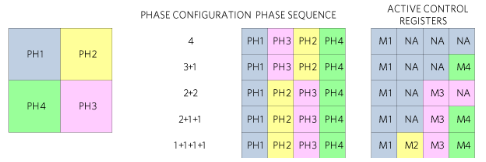
The MAX77812 is a quad-phase, high-current, buck regulator for multicore applications processors in the lat-est smart phones and tablets. The MAX77812 achieves world-class transient response with miniature PCB foot-print through the use of small inductors and output capaci-tors. Differential remote sense feedback enables tight DC and AC accuracy at the point of load. The MAX77812’s flexible architecture allows user-selectable phase configu-rations such as 4, 3 + 1, 2 + 2, 2 + 1 + 1, and 1 + 1 + 1 + 1.
Programmable current limit minimizes inductor size given the system’s actual requirements. Programmable soft-start ramp rate, rising and falling ramp rates, and startup operation provide control over inrush current as the regulator transitions between operating states. An output voltage range of 0.25V to 1.525V supports a wide range of application processors, down to the lowest power retention states.
Multifunction general-purpose inputs and high-speed serial interface provide flexible enable control of each regulator, DVS operation, and output voltage ramp rate control that enables rapid output voltage adjustment to optimize performance in all system operating states.
The MAX77812 features I2C-compatible, 2-wire serial interface consisting of a bidirectional serial data line (SDA) and a serial clock line (SCL). The MAX77812 I2C supports SCL clock rates up to 3.4MHz. The MAX77812 I2C can be configured as a 26MHz (typ) SPI interface by I2C_SPI_SEL input pin.
The MAX77812 is available in a 64-bump 0.4mm pitch WLP package with a maximum height of 0.8mm
MAX77812主要優勢和特性:
20A Maximum Output Current
2.5V to 5.5V Input Voltage Range
Output Voltage Range from 0.25V to 1.525V in 5mV Steps
±0.5% Typical DC Output Voltage Accuracy
91% Peak Efficiency at 3.8VIN, 1.1VOUT,L = 220nH (9mΩ DCR)
Enhanced Load Transient Response
Programmable Ramp-Up and Ramp-Down Slew Rate
Auto (SKIP/PWM) or Forced PWM Modes
User-Selectable Phase Configurations
Multifunction General-Purpose Inputs
Watchdog Timer Reset Input
Interrupt Output for Status and Fault Conditions
High-Speed (Up to 3.4MHz) I2C Serial Interface with an Option for 30MHz SPI Interface
MAX77812應用:
Smartphones and Tablets
Game Consoles
DSLR Cameras
Drones
Micro Processors (CPU/GPU) and FPGAs
Communication Modules
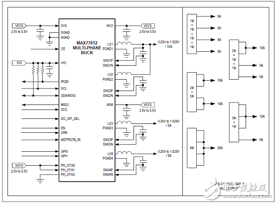
圖1.MAX77812簡化框圖
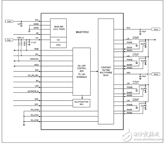
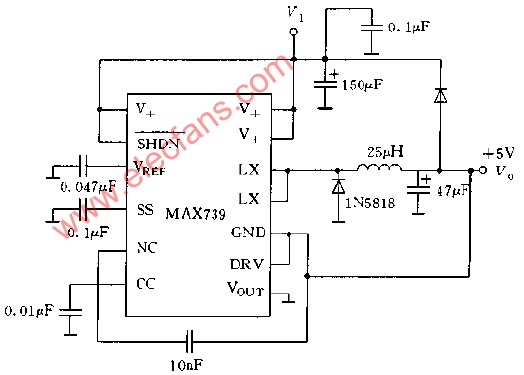
圖2. MAX77812典型應用框圖
評估板MAX77812 EVK
The MAX77812 evaluation kit (EV kit) is a fully assembled and tested printed circuit board (PCB) that demonstrates the MAX77812. The EV kit allows for easy evaluation of each feature. It supports user-programmable phase con-figuration to one of five options:
Single output in 4 phase configuration (default)
Dual outputs in 3 + 1 phase configuration
Dual outputs in 2 + 2 phase configuration
Three outputs in 2 + 1 + 1 phase configuration
Four outputs in 1 + 1 + 1 + 1 phase configuration
A Micro-B USB cable is included in the package to serve as the USB to I2C interface for easy testing. Windows?- based software provides a user-friendly interface to exer-cise the features of the MAX77812. This software offers a graphical user interface (GUI) as well as a register-based interface.
評估板MAX77812 EVK主要特性:
20A Maximum Output Current
2.5V to 5.5V Input Voltage Range
Output Voltage Range from 0.25V to 1.525V in 5mV Steps
±0.5% (typ) DC Output Voltage Accuracy
91% Peak Efficiency at 3.8VIN 1.1VOUT, L = 220nH (9mΩ DCR)
Enhanced Load Transient Response
Programmable Ramp-Up and Ramp-Down Slew Rate
Auto (SKIP/PWM) or Forced PWM Modes
User-Selectable Phase Configurations
Multifunction General-Purpose Inputs
Watchdog Timer Reset Input
Interrupt Output for Status and Fault Conditions
High-Speed (Up to 3.4MHz) I2C Serial Interface with an Option for 30MHz SPI Interface
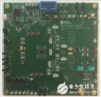
圖3.評估板MAX77812 EVK外形圖
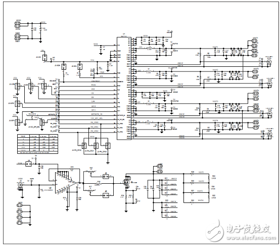
圖4.評估板MAX77812 EVK電路圖(1)
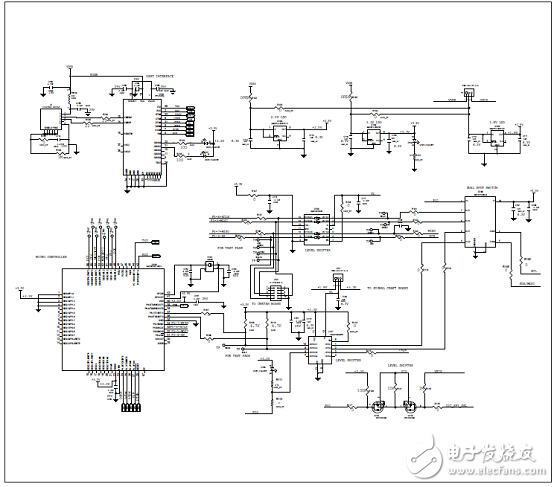
圖5.評估板MAX77812 EVK電路圖(2)
評估板MAX77812 EVK材料清單:
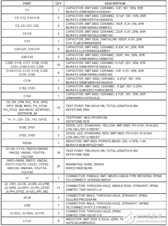
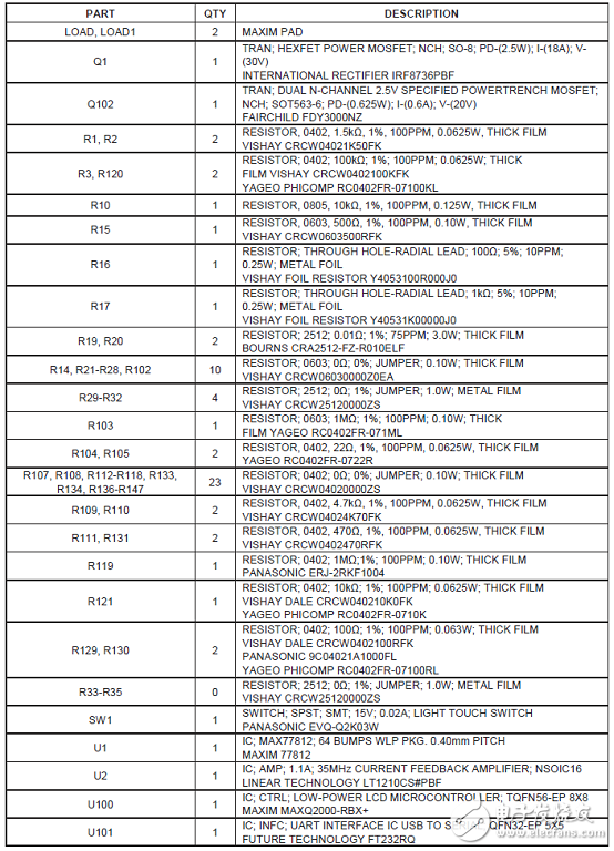
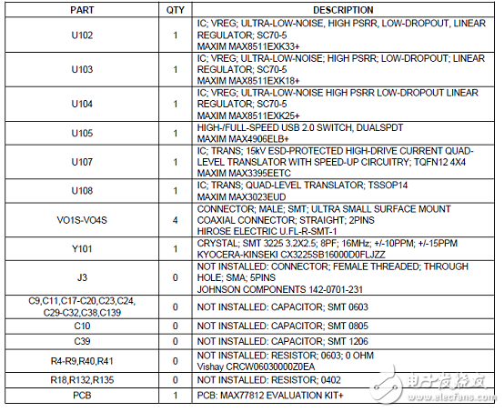
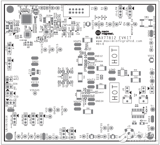
圖6.評估板MAX77812 EVK PCB設計圖(1):頂層絲印
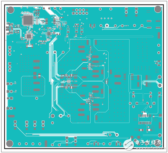
圖7.評估板MAX77812 EVK PCB設計圖(2):頂層布局
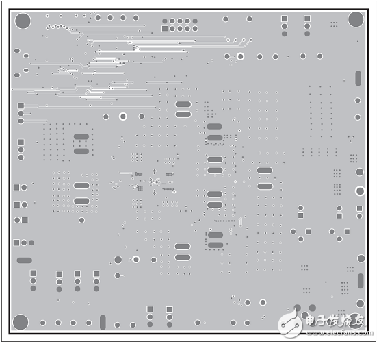
圖8.評估板MAX77812 EVK PCB設計圖(3):內層2布局
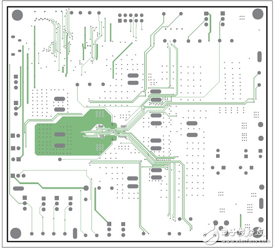
圖9.評估板MAX77812 EVK PCB設計圖(4):內層3布局
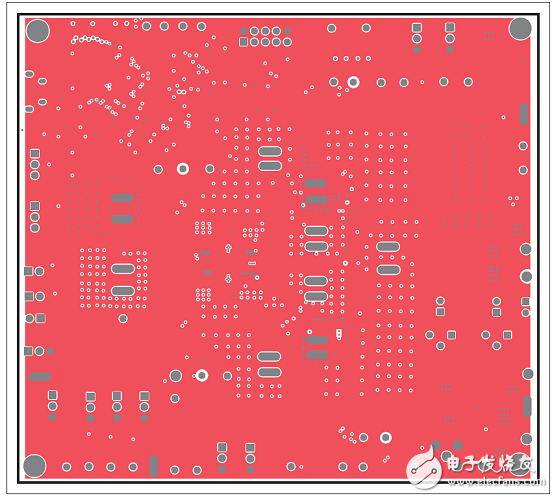
圖10.評估板MAX77812 EVK PCB設計圖(5):內層4布局
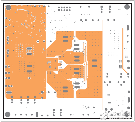
圖11.評估板MAX77812 EVK PCB設計圖(6):內層5布局
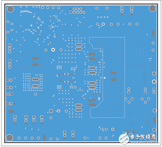
圖12.評估板MAX77812 EVK PCB設計圖(7):底層布局
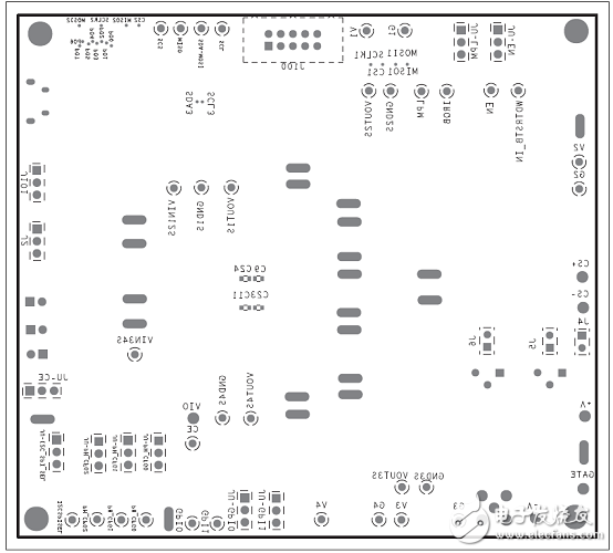
圖13.評估板MAX77812 EVK PCB設計圖(8):底層絲印


 工商網監
工商網監
評論